
Industry Coverage
Cadence Debuts Its First System Chiplet Silicon To Accelerate Physical AI Development
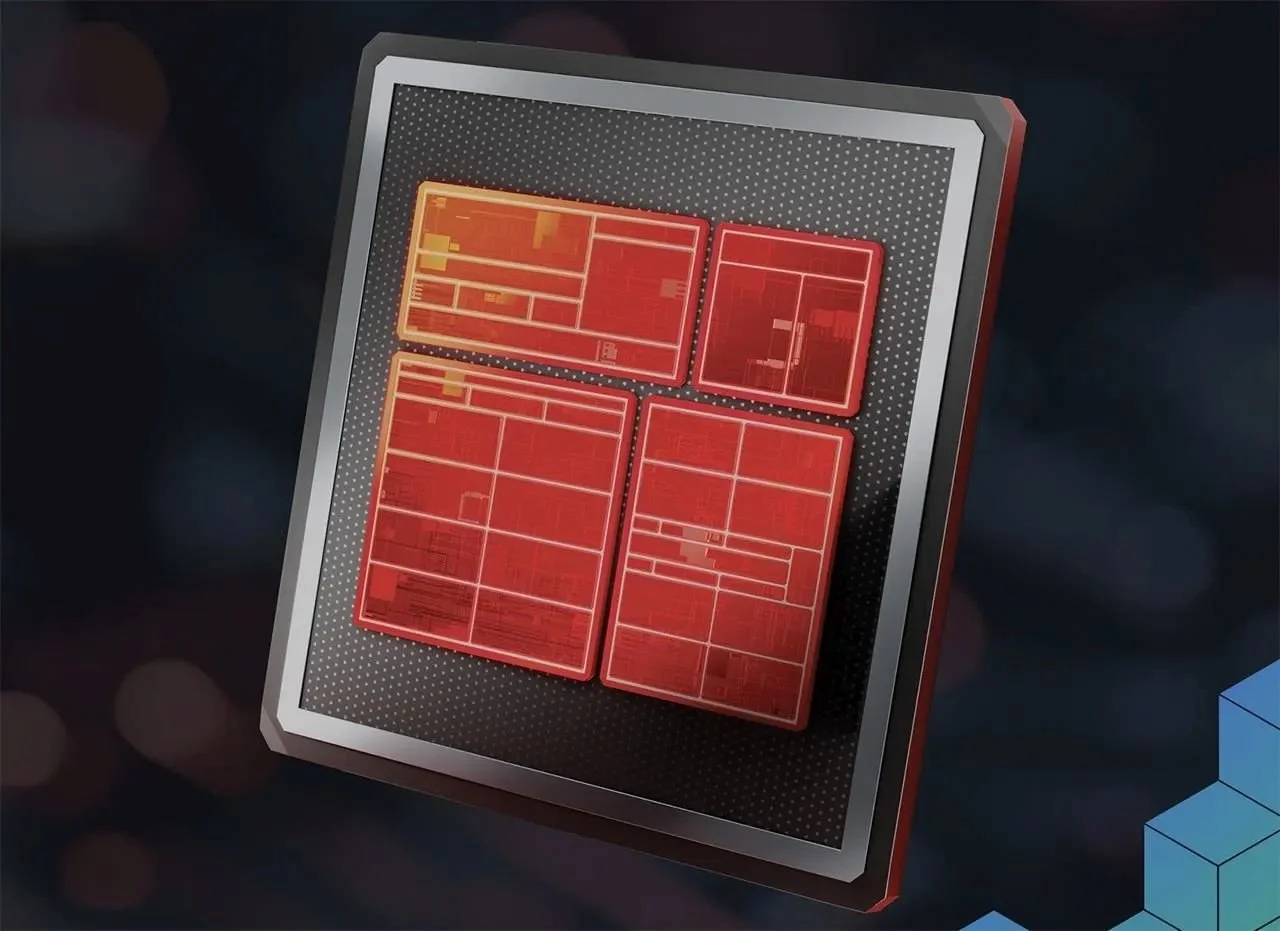
Cadence Design Systems made a major advancement with it system chiplet, that may further accelerate the semiconductor industry’s migration toward evolving chiplet-based architectures. The company detailed the successful silicon bring-up of its system chiplet architecture, which is the cornerstone of a broader chiplet ecosystem vision designed to push modular silicon platforms forward. I first wrote about Cadence’s system chiplet earlier this year…

Cadence Built A Nvidia DGX SuperPOD Digital Twin With Incredible Scale And Accuracy
In the semiconductor industry, virtually every major chip maker leverages physically accurate digital twins and simulation technologies throughout the design and manufacturing process, to gain invaluable insights into their devices, before a single wafer is prepped at the fab. When building chips, it is essentially a given that simulations and digital twins are used early and often, to ensure optimal performance, power, and area (PPA), but the same can’t be said in other industries. Even if we scale up only to the system level, for example, digital twins have been adopted by only a small fraction of companies. In this day and age of gigawatt AI factories and advanced data centers, however, it’s borderline silly to not leverage digital twins early in the design phase of complex projects.